- 氮化鎵磊晶片|GaN EPI Wafer
| 圖片 | P/N | Size | Barrier Layer AL Composition | FWHM (0002) Arcsec | Total EPI Thickness (nm) | Wafer Bowing (um) | Particle Count (ea) | |
|---|---|---|---|---|---|---|---|---|
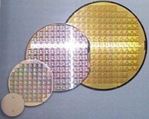 | 000S06EP01 | 6" EPI | ~750 | 4200 ±10% | +/-50um | ~500 | ||
 | 000S08EP01 | 8" EPI | ~750 | 4200 ±10% | +/-80um | ~500 |

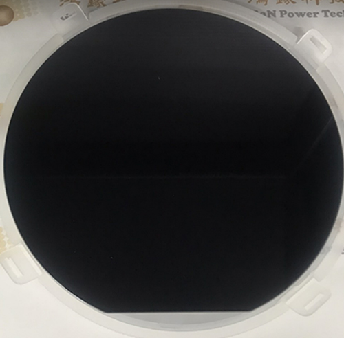
- 氮化鎵芯片|GaN Process Wafer
| 圖片 | P/N | Size | X(μm) | Y(μm) | Rds(on) Typ. (mΩ) | Ids(max.) (A) | |
|---|---|---|---|---|---|---|---|
 | 245S06PM01 | 6" Wafer | 1300 | 2050 | 220mΩ | 9A | |
| 130S06PM01 | 6" Wafer | 2000 | 2800 | 120mΩ | 18A |
- GaN FET
| Figure | P/N | Configuration | VDS(V) | RDS(on) (mΩ) | IDS(max) (A) | Package | Status | Datasheet |
|---|---|---|---|---|---|---|---|---|
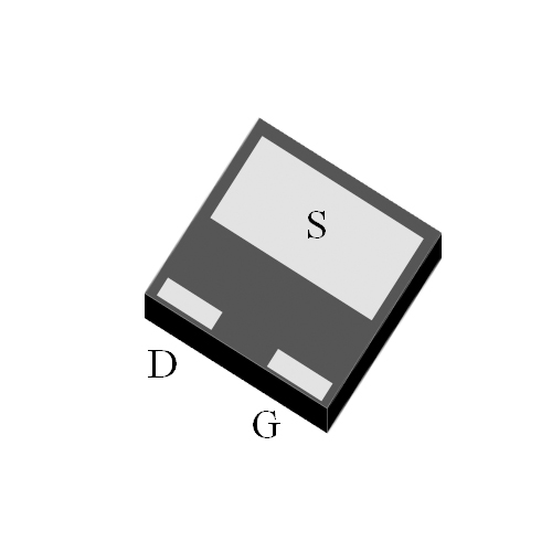 | GPT65Z3YMR | Cascode | 650V | 245mΩ | 9A | DFN8080 | Mass Production | |
| GPT65Z4YMR | Cascode | 650V | 130mΩ | 18A | DFN8080 | Mass Production | |
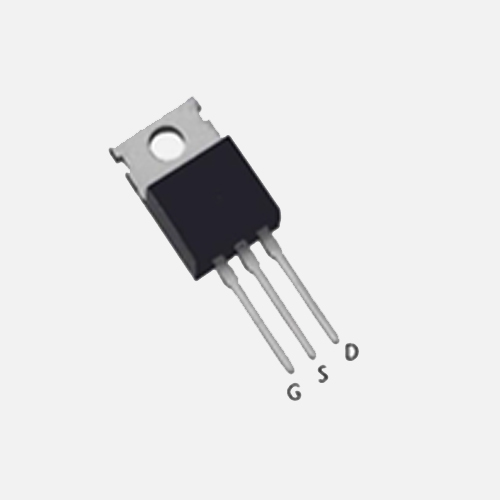 | GPT65Z4WMR | Cascode | 650V | 130mΩ | 23A | TO220 | Small Volume Production |